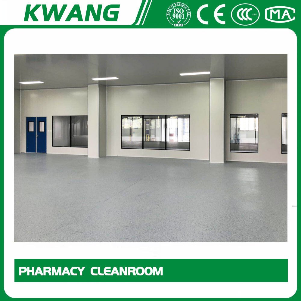
Semiconductor Cleanroom Reaches "Class 100" Level Cleanliness
The first third-generation semiconductor industrial park in Hunan province with an investment of 16 billion yuan and covering an area of 1,000 mu, as well as the first domestic silicon carbide research and development and production of the whole industrial chain production line, has a new progress. 19 January, the reporter learned from Changsha High-tech Zone, three security semiconductor project, the largest single M2B chip plant topping out, covering an area of 23,206 square meters, construction area of 52,326 square meters, steel structure large roof area 16500 square meters.
The construction side of the five companies in the construction, the project mainly contains silicon carbide long crystal, substrate, epitaxial, chip, device packaging and other plant and related ancillary facilities construction. After the project is fully completed and put into operation, it will form two production lines for the whole industrial chain of silicon carbide R&D and production, producing high-quality, low-cost, high-stability silicon carbide substrates and various devices that can be widely used in new energy vehicles, high-speed rail locomotives, aerospace and wireless (5G) communications.

After completion, the project is expected to achieve an annual output value of more than 12 billion yuan, and can drive upstream and downstream supporting industry output value is expected to exceed 100 billion yuan.
"The project mainly serves the technology-intensive semiconductor industry. Semiconductor production has high requirements for air cleanliness. The chip plant under construction has a cleanliness of 'Class 100'." Zhou Xiang, the project manager of CCB5 Third Company, said.
The so-called "Class 100" cleanliness means that the number of particles with a particle size greater than or equal to 0.5 microns per cubic foot of air does not exceed 100, which is comparable to the highest cleanliness level of the operating room standard. Lu Jianzhen, the technical person in charge of the project, said that in order to ensure the "Class 100" cleanliness, the chip plant was constructed with high precision using waffle boards (a floor board that uses holes in the floor to form return air channels) and a clean air conditioning ventilation system was established to form return air channels.
The thickness of the waffle slab in the chip factory is 70cm, which is resistant to micro-earthquakes; the waffle slab has an area of 1,410 square metres, in which 35,000 35cm diameter Kee's cylinders are poured, equivalent to 5 round holes for air exchange every 2 square metres. At that time, the chip production line will be arranged on the waffle board, and the whole workshop will use the fresh air system to ensure positive pressure and exhaust air through the return air channel of the waffle board to finally ensure the cleanliness of the workshop.

 +86 13921198925
 katherine.wang@kwangpurification.net
 8613921198925


